2026 | Professional

Customized PCB Stack-up 3D Design System
Entrant
Shenzhen Tongchuangxin Electronics Co., Ltd.- Peng Yan
Category
Conceptual Design - Technology
Client's Name
Country / Region
China
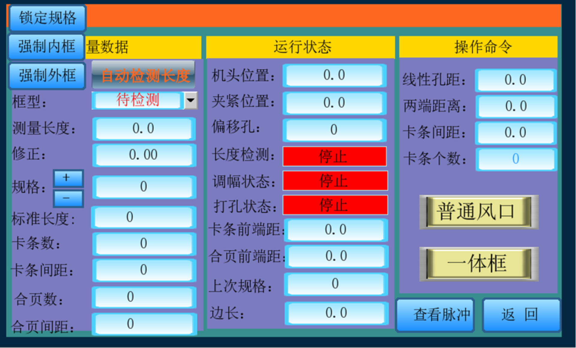
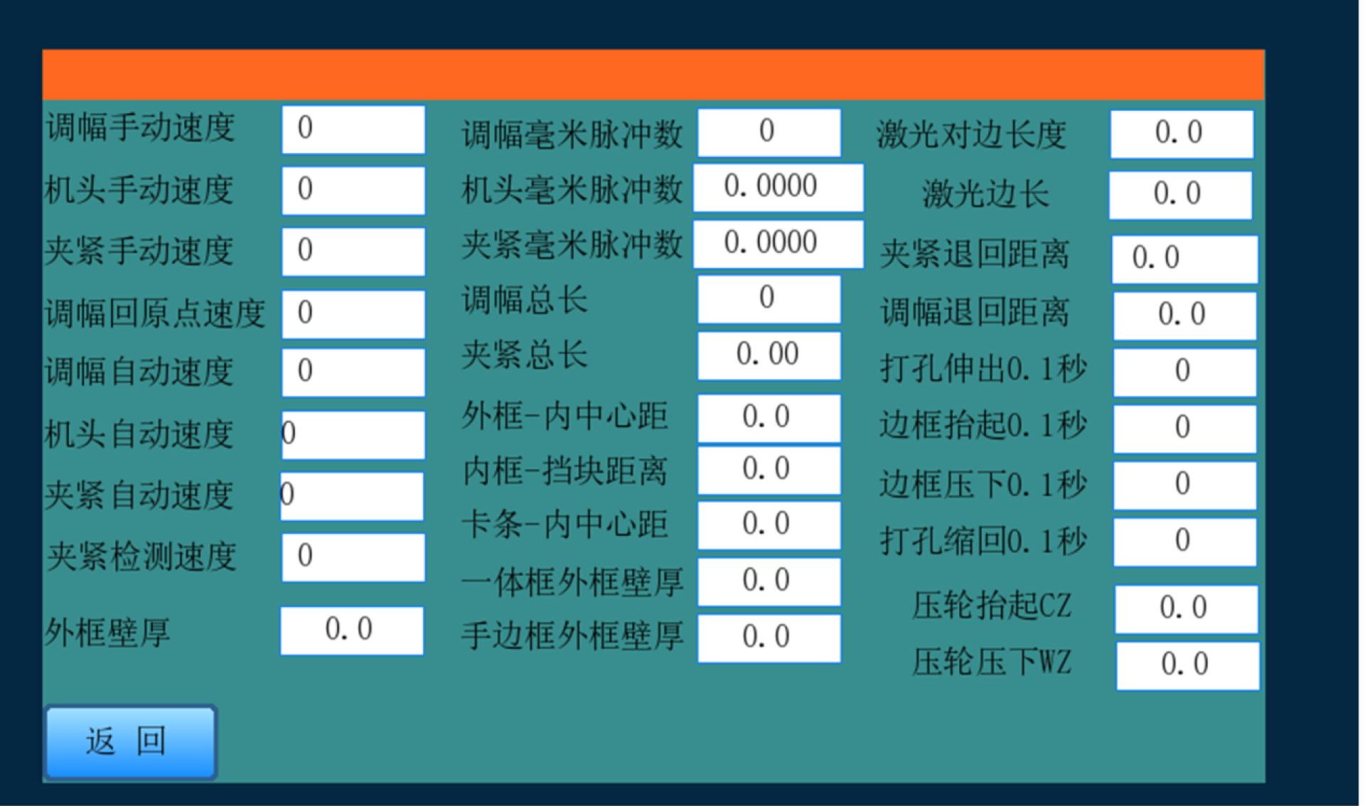
The Customized PCB Stack-up 3D Design System is a high-end professional software tailored for the field of Electronic Design Automation. It aims to address the pain point of separation and inefficiency between stack-up planning and 3D verification in traditional PCB design workflows, and seamlessly integrates parametric stack-up design, 3D physical modeling and real-time electrical performance analysis to create an integrated design and verification platform for complex PCBs such as high-speed, high-density and radio frequency types, covering the full process from stack-up scheme formulation to 3D prototype development.
This system seamlessly integrates the two key processes of stack-up structure planning and 3D spatial verification. Through its intuitive parametric interface, users can freely define the total number of circuit board layers as well as the material type and thickness of each layer, while the system automatically generates production-standard drawings and documents. Its core advantage lies in its high-precision 3D modeling capability: it can automatically construct a realistic 3D circuit board model containing all wires, holes and components based on design data, empowering engineers to conduct a comprehensive inspection of the PCB’s three-dimensional structure, identify potential issues such as component spatial interference and thermal layout flaws in advance, and thus significantly enhance the physical reliability of the design. Furthermore, it realizes intelligent linkage between design and analysis: when users adjust materials or stack-up sequences, the software can instantly evaluate the resulting impacts on key circuit performance metrics such as signal transmission quality and impedance matching, thereby mitigating risks at the design stage and reducing repeated revisions after physical prototyping.
The system effectively shortens product R&D cycles, cuts down development costs and lowers the risks of failure. It is particularly suitable for fields with stringent requirements for circuit board performance and reliability, including smartphones, automotive electronics, industrial control systems and communication equipment, and has emerged as a core tool in the modern electronic product R&D workflow.
Credits
Entrant
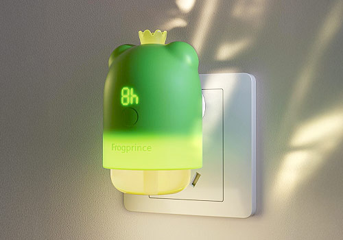
Frog Prince (Fujian) Baby & Child Care Products Co.,Ltd.
Category
Product Design - Baby, Kids & Children Products

Entrant
Ping Chen Design
Category
User Experience (UX) Design - Health / Fitness / Wellness
Entrant
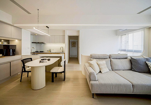
Wan Mei Interior Design
Category
Interior Design - Residential
Entrant
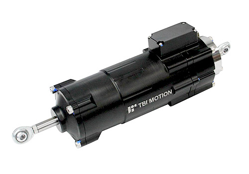
TBI MOTION TECHNOLOGY CO.,LTD
Category
Product Design - Industrial Equipment, Machinery & Automation